

If for any reason we need to work on PCBs after components have been assembled then it’s vital that we do so without damaging them. Electrostatic discharge, or ESD for short, occurs when two objects or surfaces release static energy. There is a high risk of electrostatic charges developing when working with printed circuit boards which have been populated with components. Simply walking across a carpet in normal clothes generates around 3000 volts, with as little as 10 volts being enough to damage a PCB component.
Electrostatic discharge develops when two materials rub together so that one becomes positively charged and the other negatively charged. The positive material contains an electrostatic charge which is then transferred onto another surface to produce an ESD event.
How does ESD damage PCBs?
When an ESD event occurs, heat is generated which can melt parts of the components causing them to fail. Even if the heat damage isn’t enough to make the components malfunction initially, it can significantly reduce the lifespan of the device in which the board is fitted.
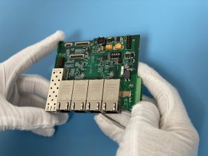
An electrostatic discharge event is likely to happen if a work surface, flooring, chairs or clothing are predisposed to cause static. For example, if a work surface is made of plastic, or a wood/vinyl chair is being used, or non-conductive shoes are worn.
This is why we have installed a dedicated ESD-safe production environment, more commonly known as an ESD Protected Area (EPA), where we have invested in a range of measures to keep boards free from static and subsequent malfunction.
Our ESD Protected Area
An ESD Protected Area is designed to limit the static electricity on all materials within that zone. Anyone who is working there should be connected to ground, as should any conductive equipment or surfaces within the area.
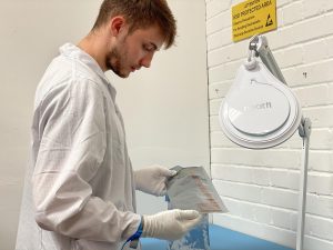
In order to protect PCBs and the components populated on them, we have introduced the following equipment:
- Wrist Straps
- Anti-static mat
- Electrostatic meter
- Protective Clothing
Testing static levels
The ESD meter is used to ensure that the person inspecting the boards is properly grounded, as it measures how much ESD is being produced. It displays a green or red light to indicate whether it is safe to work on the boards or not.
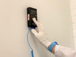
The meter must be used to check static levels before any member of staff handles the boards.
Protecting customers’ boards
Using special wrist straps ensures that any static is grounded and components on the PCB aren’t compromised.
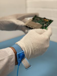
The measures we have taken to ensure that boards are handled safely will give customers confidence that we can work on their products without damaging components.
If you’d like to talk to our team about any aspects of PCB manufacture and our aftercare service then call our team on 01903 231901 or email sales.uk@starteam.global.